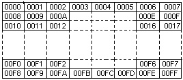
Fig. 1. Memory addresses of bytes mapped onto TV screen in sample program.
Fig. 1. Memory addresses of bytes mapped onto TV screen in sample
program.
to work in conjunction with the new graphics IC. This allows you to display any 256-byte segment of memory on a CRT monitor or TV receiver. The output of the new chip is a 1-volt composite video/sync signal.
The selected segment of memory appears on-screen as an array of small squares that represent individual memory bits. If a memory bit is a 1, the appropriate square will be white, while if a bit is a 0, the square will be dark. Changing the bit pattern within the memory will change the pattern that appears on-screen. You can store several different bit patterns (pictures) in memory and, [43]
| Label | M | Bytes | Comments |
|---|---|---|---|
| Start | 0000 | 90 B1 B2 | R1.1,R2.1=00 |
| 0003 | B3 B4 | R3.0,R4.0=00 | |
| 0005 | F8 2D A3 | R3.0=(main) | |
| 0008 | F8 3F A2 | R2.0=(stack) | |
| 000B | F8 11 A1 | R1.0=(interrupt) | |
| 000E | D3 | P=3 (go to main) | |
| Return | 000F | 72 | restore D,R2+1 |
| 0010 | 70 | restore XP,R2+1 | |
| Interrupt | 0011 | 22 78 | R2-1,save XP @ M2 |
| 0013 | 22 52 | R2-1,save D @ M2 | |
| 0015 | C4 C4 C4 | no-op (9 cycles) | |
| 0018 | F8 00 B0 | ||
| 001B | F8 00 A0 | R0=0000(refresh ptr) | |
| Refresh | 001E | 80 E2 | D=R0.0 |
| ---- | ------ | 8 DMA cycles (R0+8) | |
| 0020 | E2 20 A0 | R0-1,R0.0=D | |
| ---- | ------ | 8 DMA cycles (R0+8) | |
| 0023 | E2 20 A0 | R0-1,R0.0=D | |
| ---- | ------ | 8 DMA cycles (R0+8) | |
| 0026 | E2 20 A0 | R0-1,R0.0=D | |
| ---- | ------ | 8 DMA cycles (R0+8) | |
| 0029 | 3C 1E | go to refresh (EF1=0) | |
| 002B | 30 0F | go to return (EF1=1) | |
| Main | 002D | E2 69 | X=2,turn TV on |
| 002F | 3F 2F | wait for IN pressed | |
| 0031 | 6C A4 | set MX,D,R4.0=toggles | |
| 0033 | 37 33 | wait for IN released | |
| 0035 | 3F 35 | wait for IN pressed | |
| 0037 | 6C | set MX,D=toggles | |
| 0038 | 54 14 | set M4=D,R4+1 | |
| 003A | 30 33 | go to M33 |