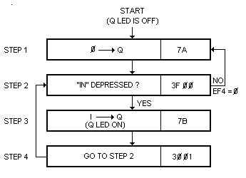
Fig. 7. Program turns on Q-LED when INPUT switch is operated.
cremented by one so that input bytes will be sequentially loaded into RAM locations. Line SC1 goes high during the DMA IN cycle so that the control circuits know when the input byte has been stored in the RAM.
Depressing and releasing INPUT switch S12 sets flip-flop IC12 (Fig. 5). The ~Q output of this stage goes low, causing the required low on the ~DMA~IN line. The 1802 responds to this request with a memory-write cycle during which SC1 is high. During this cycle, ~MREAD is high and, since LOAD switch S2 is also ON, the N2/LOAD signal causes gate IC10C to go high, gating the switch input byte to the data bus and storing it in memory. When SC1 goes high, it also resets IC12, which causes ~DMA~IN to return to its high state. The computer then waits for the next switch input byte and LOAD switch operation.
Following each DMA IN cycle, the 1802 holds the A0 through A7 lines at the address of the byte just stored in the RAM. ~MREAD is also held low while waiting for the next input byte. This means that the previously loaded byte is being gated to the bus (from the RAM) while waiting for a new byte. This bus byte is continuously clocked into the hex display, since the LOAD switch is holding IC10B open.
A sequence of program bytes can be loaded into the RAM starting at M0 = M(0000) by setting the LOAD switch to the ON position, with the RUN switch set to OFF. Set the eight input switches, S4 through S11, to the desired byte code (in hexadecimal) and depress the INPUT switch to store the byte in the RAM. The value of this byte will be displayed with the hex displays IC6 and IC7. Repeat this procedure for each byte to be loaded. Setting the LOAD switch to OFF puts the 1802 back in the reset state where R0 = 0000, P = 0, X = 0, and Q = 0. If you wish to see what is stored in memory, set MP (memory-protect) switch S3 and the LOAD switch to ON. Now, each time you operate the INPUT switch, successive bytes in the RAM, starting with M(0000), will be displayed.
To change a byte, proceed to the byte just before the one to be changed. Flip the MP switch to OFF, set the input toggle switches to the hex value of the new byte, and depress the INPUT switch once. This new byte will be displayed and stored in the RAM at the location following the byte at which you stopped. Place the MP switch in the ON position. You can now continue to operate the INPUT switch to sequence through the RAM without modifying the bytes in memory.
To start the executive cycle of a program, set both the LOAD and RUN switches to OFF (to reset the 1802). Then set the RUN switch to ON. The program counter is always specified by the hex digit in register P, which can be set to zero by reset so that the program counter will always initially be R0. Set R0 to 0000 by resetting so that instruction fetching, or program execution will always begin at M(0000). Instructions will continue to be fetched from the RAM and executed until the RUN switch is set to OFF, resettting the computer. Make sure that the MP switch is OFF when running programs so that computer operation is not inhibited.
Construction Notes. Hardware assembly is relatively simple, permitting the project to be put together with ordinary perforated board with 0.1" (2.54-mm) hole spacing and IC sockets, using either Wire Wrap® or a wiring pencil. (See photo.) The perf board measures 5½"L × 4"W (14 × 10.2 cm) and is supported on a base made up of lengths of ¾" × 3/8" (19.1 × 9.5) pine. A sheet of thin aluminum provides the support for the eight toggle-type data switches. The LM309 voltage regulator IC (IC13) is mounted on a 1¼" × ¾" × 1/8" (31.6 × 19.1 × 3.2-mm) piece of aluminum to serve as a heat sink.
Do not mount the IC's (except the display devices) in their sockets until after all wiring is complete. Socket, switch, and component layout should be roughly the same as shown in the photo. Be sure to locate the crystal close to pins 1 and 39 of the microprocessor's socket. Then wire the circuit in accordance with the schematics in Figs. 4 and 5.
Any crystal with a frequency of between 1 and 2 MHz can be used in the Elf, or you can substitute a simple 555 or CMOS oscillator with a 5-volt signal swing between pin 1 of the 1802 and circuit ground, in which case, you will have to omit XTAL, C3, C4, and R11. There is no lower limit to the clock frequency, but most of the sample programs discussed in this series of articles are based on a clock frequency between 1 and 1.8 MHz.
Displays IC6 and IC7 are relatively expensive hex devices. They are the only TTL devices in the computer and, as a result, draw most of the power required by the circuit. If you wish to economize, you can substitute ordinary LED's for the displays. (Next month, we will discuss how to make the substitution.)
An inexpensive 9-volt, 350-mA dc battery eliminator, like those used as battery charger/eliminators for calculators, can be used to power the Elf.
When the computer is completely assembled, use a dry-transfer lettering kit to label all switches and positions. IC socket locations, and pins 1 of all sockets. Then, exercising the usual safety procedures for handling MOS devices, install the integrated circuits in their respective sockets.
Coming Up. In future articles, we will provide more programs as well as methods of adding other types of inputs and relay-control output circuits. We will also detail how to save programs in battery-powered COSMOS RAM's and describe a simple operating system that lets you read/write any memory location and inspect general register contents for program debugging purposes. Memory expansion, hex keyboard input, and an inexpensive video graphics display are other subjects we will cover in detail. •
[33] [34] [35] [36] [37] [38]