Sorry about the pictures, they're a little fuzzy
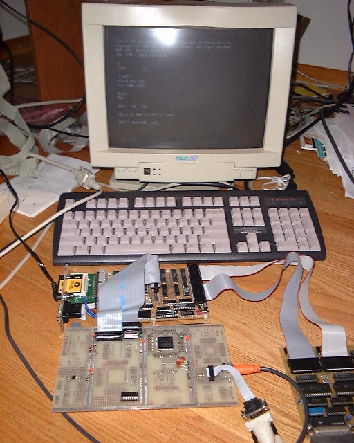
Here's the running prototype (front center) with a VGA monitor and a PS/2 keyboard. The board on the lower right is Bob's EPROM emulator (actually his, I borrowed it ;-))
See next picture for a more detailed description of the prototype.
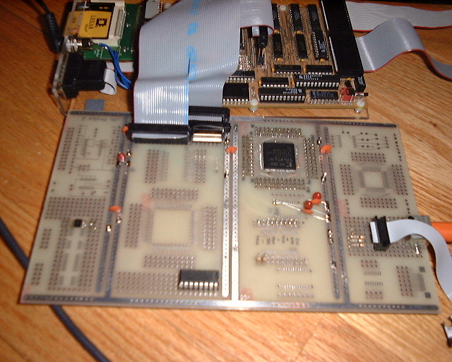
I used an SMT prototyping board that I had done for another project. It has 'breakout' patterns for various SMT footprints to pads for wire-wrap posts. In this case I used very few of them...
Left out of this prototype is the entire memory subsystem that duplicates Bob's ramdisk card, since it is relatively straightforward. Also left out is the CompactFlash interface. I wanted to test some of the FPGA related stuff with this, specifically:
- Downloading the FPGA configuration data (128KB) via the CPU
- The PS/2 and VGA interface
- The KL8JA serial ports (at TTL levels)
What you see here is: the 3.3v regulator on the left, the connection to the
SBC6120 at the back (hidden behind that is a 2.5v regulator), a clock
oscillator, the FPGA and in front an address decoder. All that's left is a
few connectors, caps and resistors, yet...
It's a fully working VT52 terminal, plus all that other stuff!
Here is a mock-up of how the circuit will look mounted to the SBC6120.
The back edge has connectors for the parallel printer, keyboard and VGA display. The front edge has the CF card sticking out. The three serial ports are on the three headers in the top right-hand quadrant. The two headers in the lower center carry the CPU data bus and 36 I/O pins from the FPGA.
Along the top left edge you see the 4 RAMs that duplicate the ramdisk board, plus a flash ROM that holds the FPGA configuration file and the extensions to BTS6120 for the I/O board.
In the default configuration, the I/O pins are individually controllable for input or output, but there is a significant amount of free logic in the FPGA that could be used to interface high-speed peripherals or a front panel implementation though these lines.
The board has gotten a little more crowded than it was, because of the new features, and because the data bus to the SBC6120 is now buffered to ensure that it doesn't overload the CPU's driving capacity.
Also added (although not coded into the FPGA yet) is a speaker for the terminal bell and a clock/calendar chip. OS/8 has no particular concept of time, but a device driver might at least update its month and day so that file dates are correct.
BTW, I found many of the connectors and the battery holders for free by raiding the dead motherboard pile at my local PC clone building shop. You also might find the 32.768 KHz crystal used by the clock chip.
Another thing worth mentioning - Parts can be omitted if not needed, e.g.the
serial ports, the parallel port, the calendar chip, the CompactFlash socket,
even the RAMs for
the ramdisk and the battery backup parts associated with them. The only
core components are the FPGA, the flash ROM and their support components.