These notes are in addition to the Assembly section in the main manual.
Please read this whole document, including the Errata
section below before starting!
Use the parts list to identify the ICs; many of them are different sizes and will only fit in their proper positions. A few minor substitutions were made:
1. SRAMs are Samsung K6T64008 (was Toshiba TC554001AF)
2. RS232 transceiver is Sipex SP208CT (was MAX208CWG)
3. Capacitors C1 & C2 can be any value 10uF and up; the ones supplied are 47uF.
The chip resistors are marked (and have very fine printing on them as well). There are two kinds of chip capacitors, large and small, which have no markings. They both are 0.1μF, but the larger ones are used for the RS232 transceiver.
Read the errata section below before starting construction!
Again, it is very important that the fine pitch parts be aligned as well as possible before more than one or two pins are soldered down! It is very difficult to recover from a mistake in this area, and easy to pull traces etc. while trying to.
Be careful not to switch the two regulators. The text on the board matches the last two digits of the part number.
Make sure that the speaker is mounted with the (+) symbol on the band matching the one printed on the circuit board.
A 2x40 pin header is supplied for the expansion connectors (two 2x13 connectors), which needs to be cut down. Cleanly snapping a 2x header strip is a little tricky; I would pull the two pins past where it will be cut (i.e. the 14th from each end), and then carefully clip it in that empty section with a pair of diagonal cutters.
The orientation of the larger capacitors C1 and C2 is a little unclear - the banded side should be towards the center of the PCB.
The orientation of the smaller (SOIC-8) ICs is unclear - all ICs are placed with pin 1 on the lower left for horizontally oriented parts and on the upper left for vertical ones.
A pair of small screws to secure the CF socket are supplied. Make sure that the tabs towards the front of the socket are soldered down to their respective pads, too. I have found that the easiest way to mount this part is to carefully align it and solder down a couple of pins that look straight (since they arrived loose, some of the pins tend to be a bit askew), then solder the tabs down, and then using a dental pick carefully adjust the remaining pins so that they are all straight and even. Finally, solder them all down and check for bad joints the usual way.
Don't forget the 8 bypass capacitors on the bottom of the board!
Underlined text below are things that are best done during construction, like not soldering down certain pins.
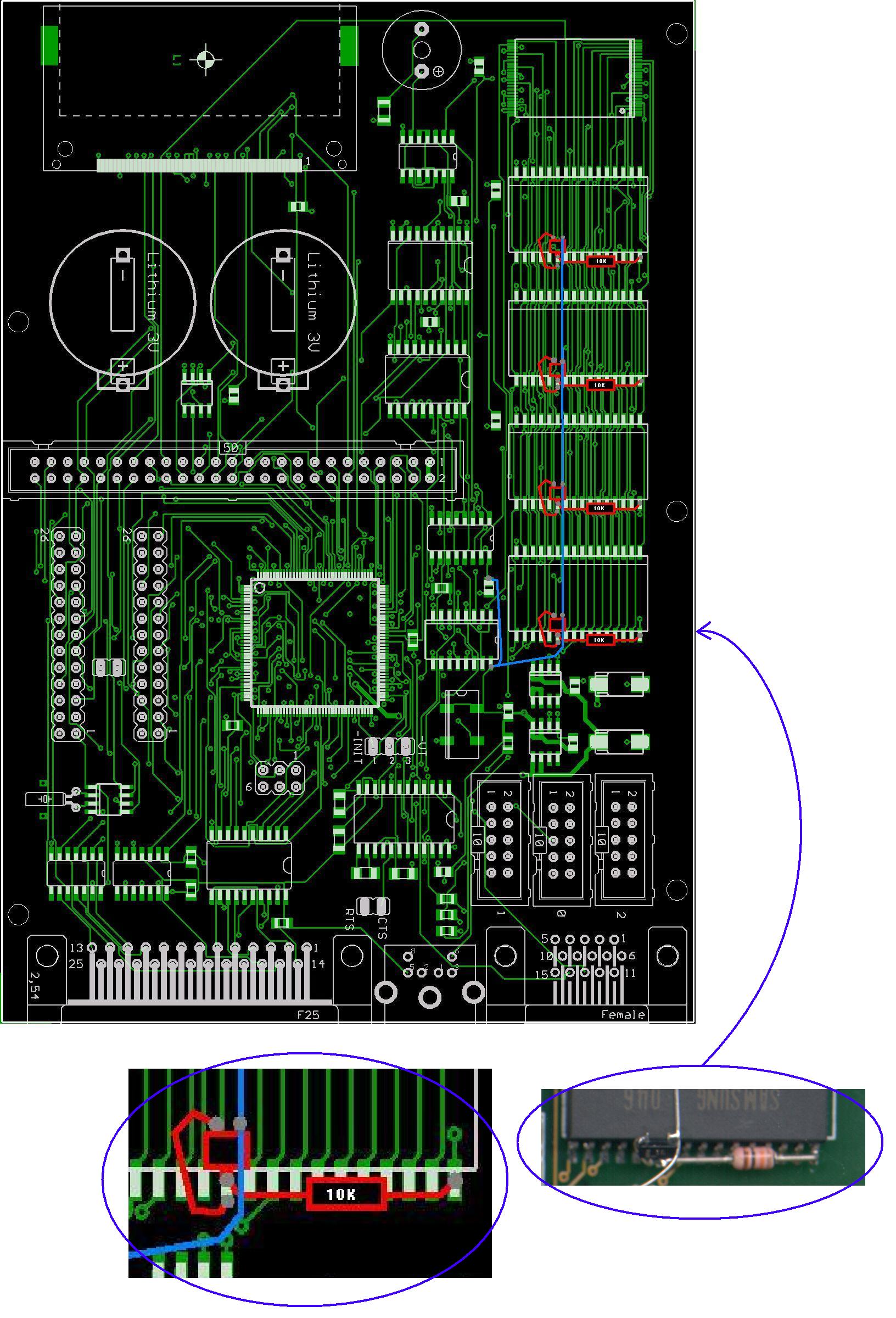
The revision A board has two known problem areas, both of which can be fixed by following the directions here.
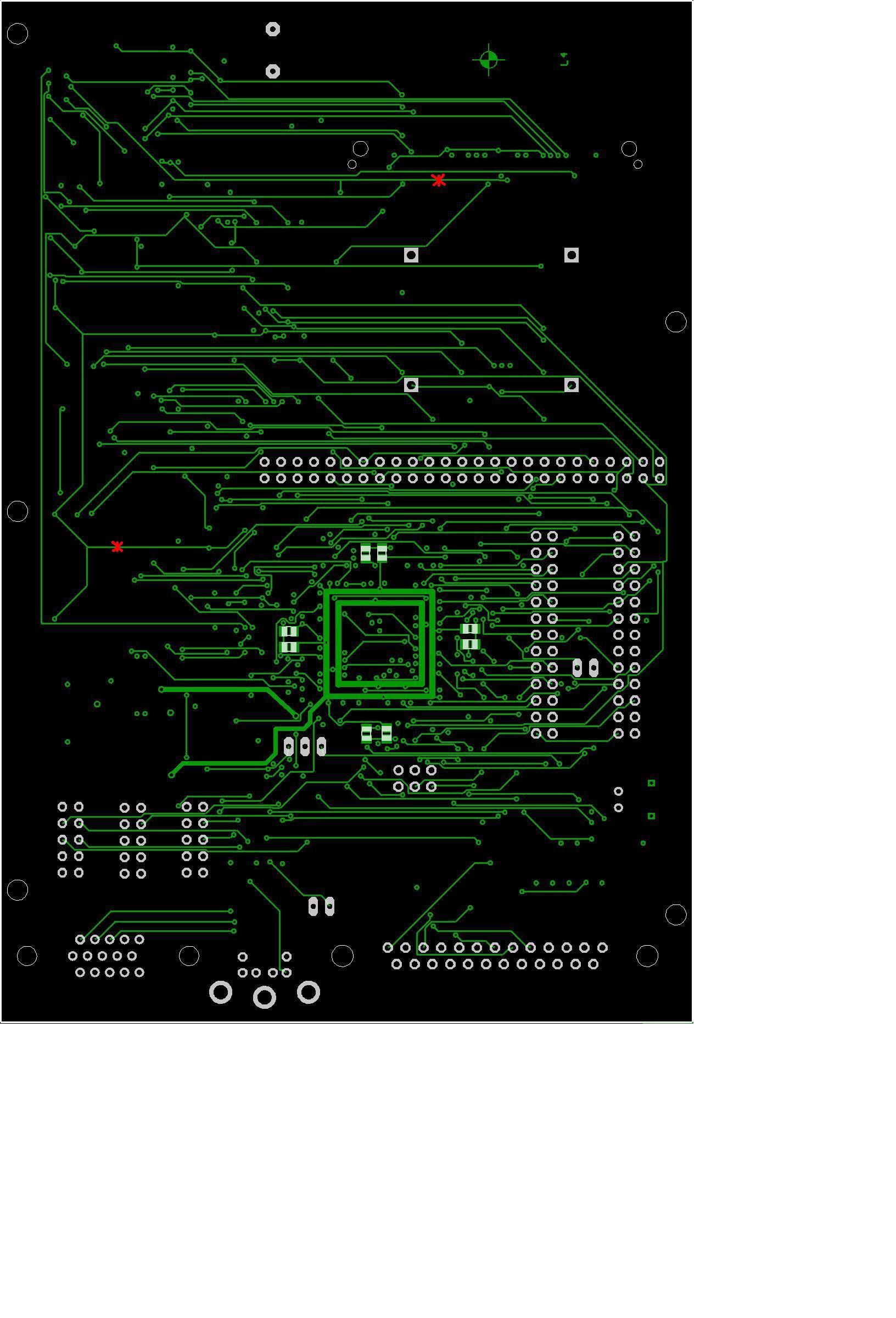
The first fix is relatively simple – the reset signal to CF card causes some problems. The fix for this is just to cut the trace on the board, and the card will be reset by software. This cut will already be made on the boards you receive, and is shown on the board images below.
The second fix is more complicated. The battery backup design for the NVRAM is faulty; current paths into the un-backed-up part of the circuit drain the batteries more quickly than desired. Two fixes were devised for this problem. The first fix is easier to apply, but is not quite as clean-looking. The parts for this one are included in the kit contents, but I will be happy to supply the parts for the second one.
Both fixes require that pin 6 of IC14 (BQ2201) be lifted and not connected to the pad below it.
This process is a lot easier to understand if you open the high-resolution top image to look at while you read it.
Here are the details - click on top or bottom picture for high resolution view. On the front side view, the changes are shown in blue and red. On the back side view, the two trace cuts are shown as red crosses.